Quality testing of microchips
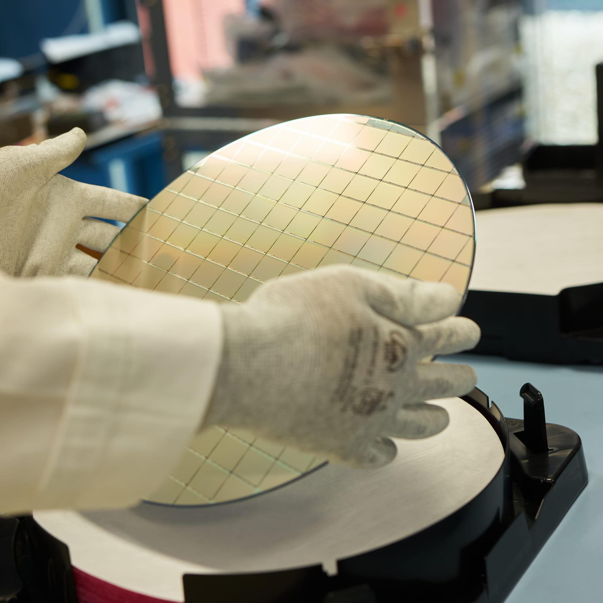
In this project I've developed the data-analysis and visualisation system for quality-assurance of CROC readout chips. About 47K of these chips have been manufactured by TSMC using the 65nm CMOS process to be bump-bonded to the pixel sensors of the CMS Tracking Detector. The chips are lithographically printed on 300mm wafers with 136 dies per wafer, out of which a certain fraction of chips typically have defects.
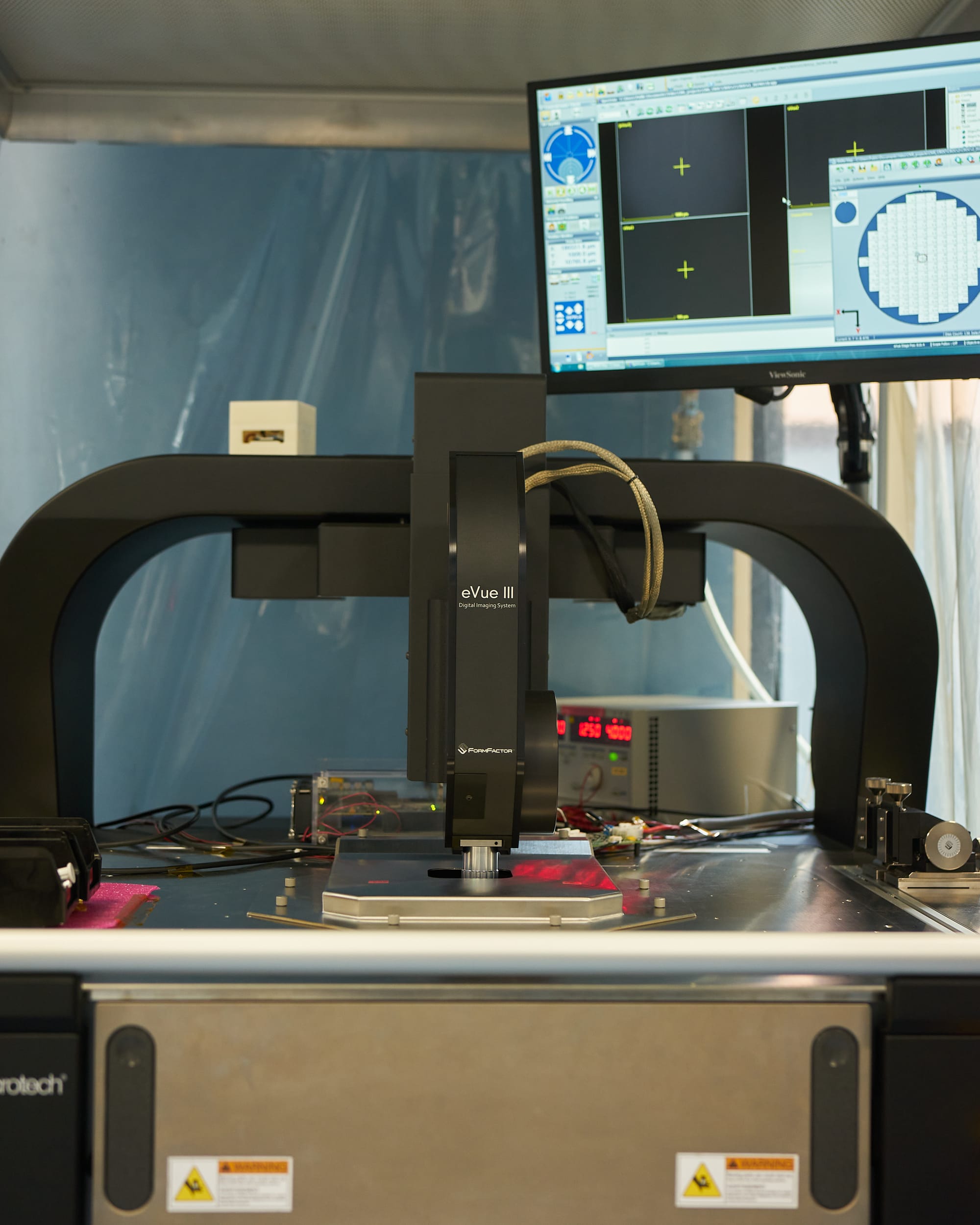
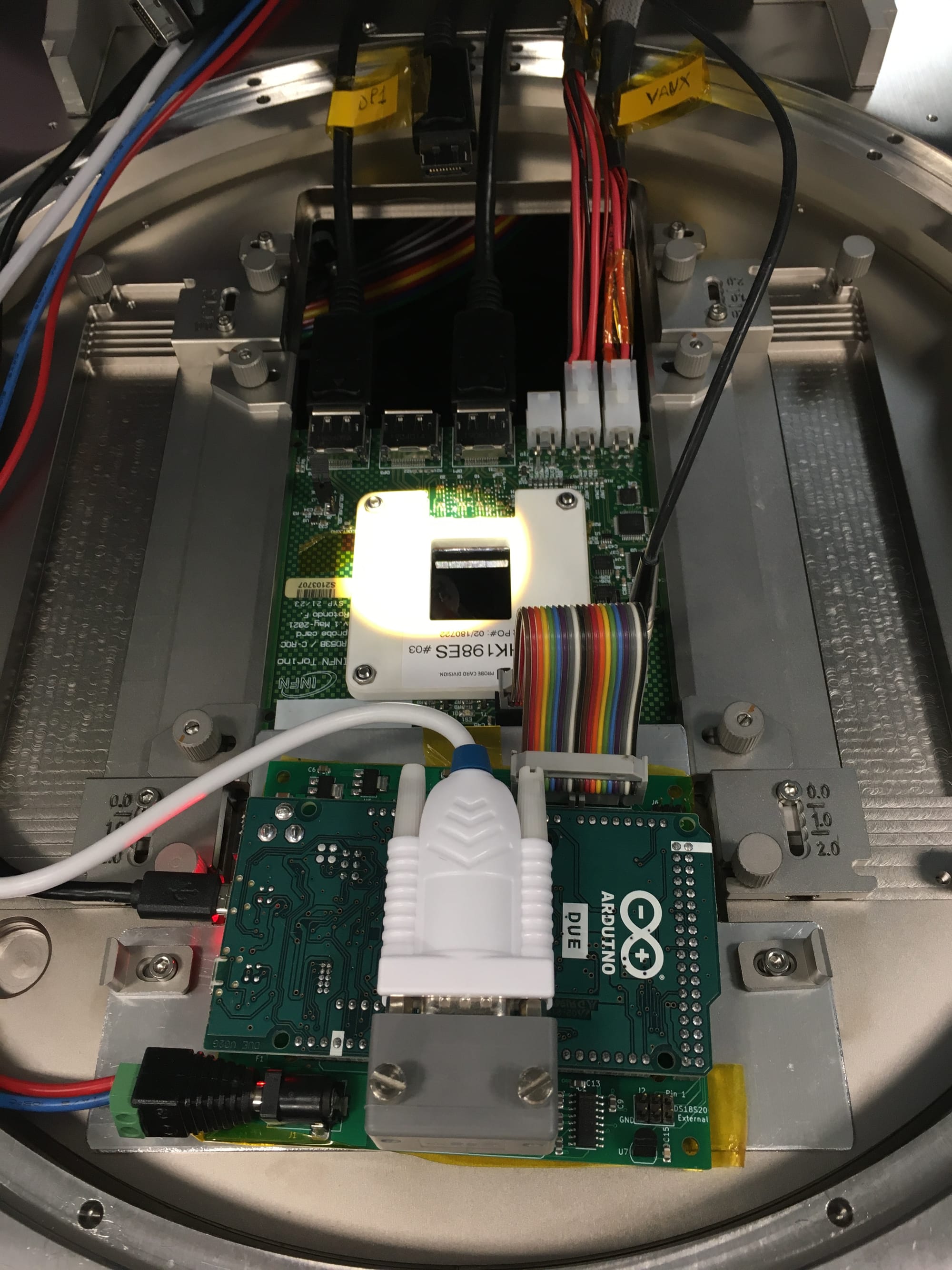
As the first step in the process of selecting high-quality chips we test them one by one directly on the wafer, before dicing and bump-bonding them to the actual sensors. This is done using a probing station equipped with a motorised microscope for precise positioning, and custom electronics (including a probe card) that has microscopic pins that touch the wire-bonding pads of a chip. The whole system allows to power a chip and to communicate with it, testing a wide range of its functions to decide if it can be used for the later production stages.
› More about the CROC chip
CROC chip (2x2cm in size) has been custom designed by the RD53 Collaboration to withstand extreme levels of radiation (up to 1 Grad of total ionising dose) that it will be exposed to at the HL-LHC (High Luminosity Large Hadron Collider). Its layout matches that of the Si sensors, using rectangular 25x100um pixels arranged into 336 rows by 432 columns, resulting in a total of 145,152 pixels in a single chip.
Each pixel has its own circuit with an analogue and digital readout, as well as a chip-wise blocks for powering and data processing, including zero-suppression and data compression before sending it out to the external part of the data-acquisition chain. This allows it to operate at the extremely high 40 MHz rate, in sync with beam collisions at the HL-LHC that will repeat every 25 ns.
Pixels are rectangular, not square, in order to provide finer pitch in the bending direction of charged tracks contained in the magnetic field of the CMS detector. The curvature of a track is used for reconstructing its momentum and has therefore higher priority than its position along the beam.
Much more technical information about the chip is available in the RD53C-CMS manual (114 pages).
Our group at INFN Torino was in charge of building a semi-automated quality-assurance system capable of testing one wafer a day. Manual human intervention was only expected every morning for review of the test results, unloading/loading of the wafers into the probing station and maintenance of the cleanroom. I was in charge of building the system for automated analysis of the test results to streamline the quality-grading process.
Main objectives
A long list of measurements, tests and calibrations are performed for every chip, including power consumption, data processing, pixel addressing, occupancy and noise levels, multiplexers, ring oscillators, temperature sensors, ADCs and DACs, and more. In total there are 300+ individual tests executed for every chip, which have been gradually implemented over time, as we were gaining more experience with the chips from different production batches.
Flexibility
Like most things in our field, we work with relatively small productions that require custom and flexible solutions easily adaptable to any changes that arise in the process. This means that the quality-grading logics had to be defined in a way that is easy to implement, easy to interpret and easy to adjust.
Chip-level updates
There are many external factors that can degrade the quality of such tests or make them impossible, such as oxidation on the probe-card needles, wrong alignment of the wafer, lithographic defects, mechanical damage or dust, faulty electronics or measurement equipment, etc. To avoid wasting time on tests that aren't working properly, the analysis workflow has to support gradual update of the analysis results after every tested chip. This allows to abort the testing procedure within the first few hours without letting the probe station touch all the chips of the wafer.
The micro-needles of the probe-card leave dents in the metal pads of the chip. Therefore, the number of times they get in contact should be kept as low as possible to keep the pads in a good shape for wire bonding during the module assembly.
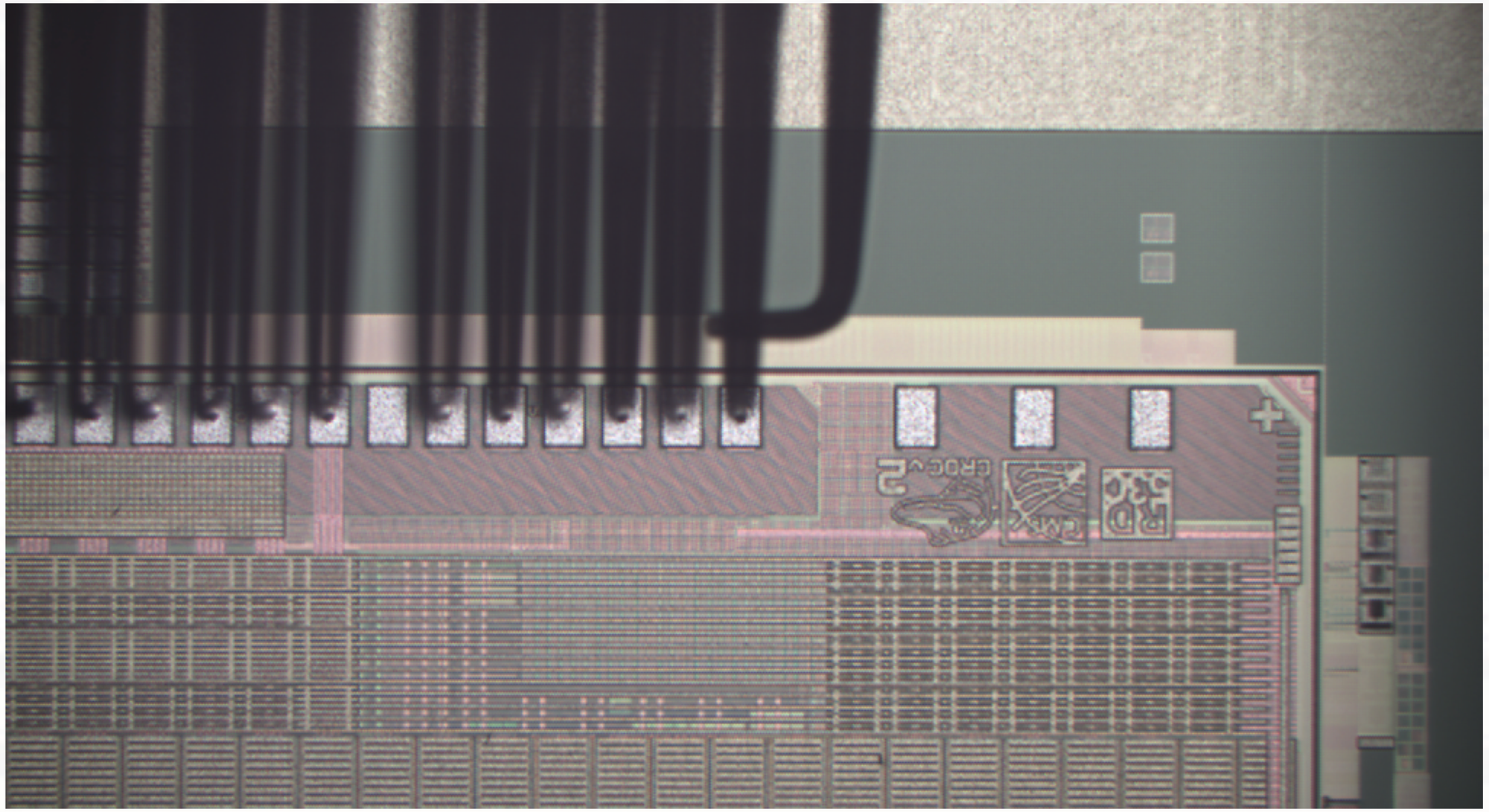
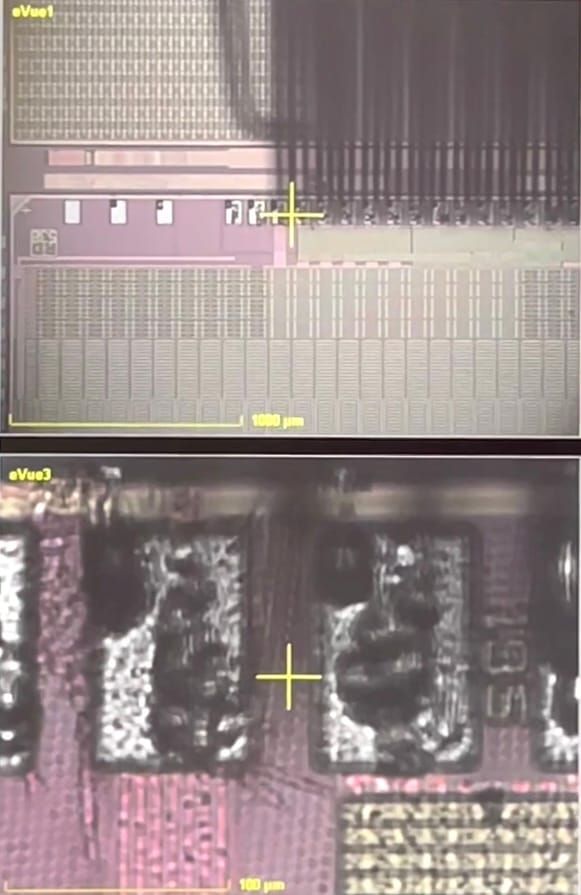
View on the CROC chip structure under the microscope showing untouched (left) and touched pads (right) obstructed by the needles of the probecard
Fast processing
Along the way we've hit a number of limitations in the data-acquisition firmware, which required collection of hundreds of megabytes of raw data from each chip to further process it during analysis, such as threshold and noise scans across all the pixels in a chip. This made the processing time critical for maintaining the intended rate of 1 wafer per day.
Scope separation
From the start we knew that we have to differentiate between critical tests that define the actual quality of the chip and complementary tests that we use for understanding the behavior of the chip and of the testing equipment itself, including various cross-checks and calibrations.
Visual and numerical presentation
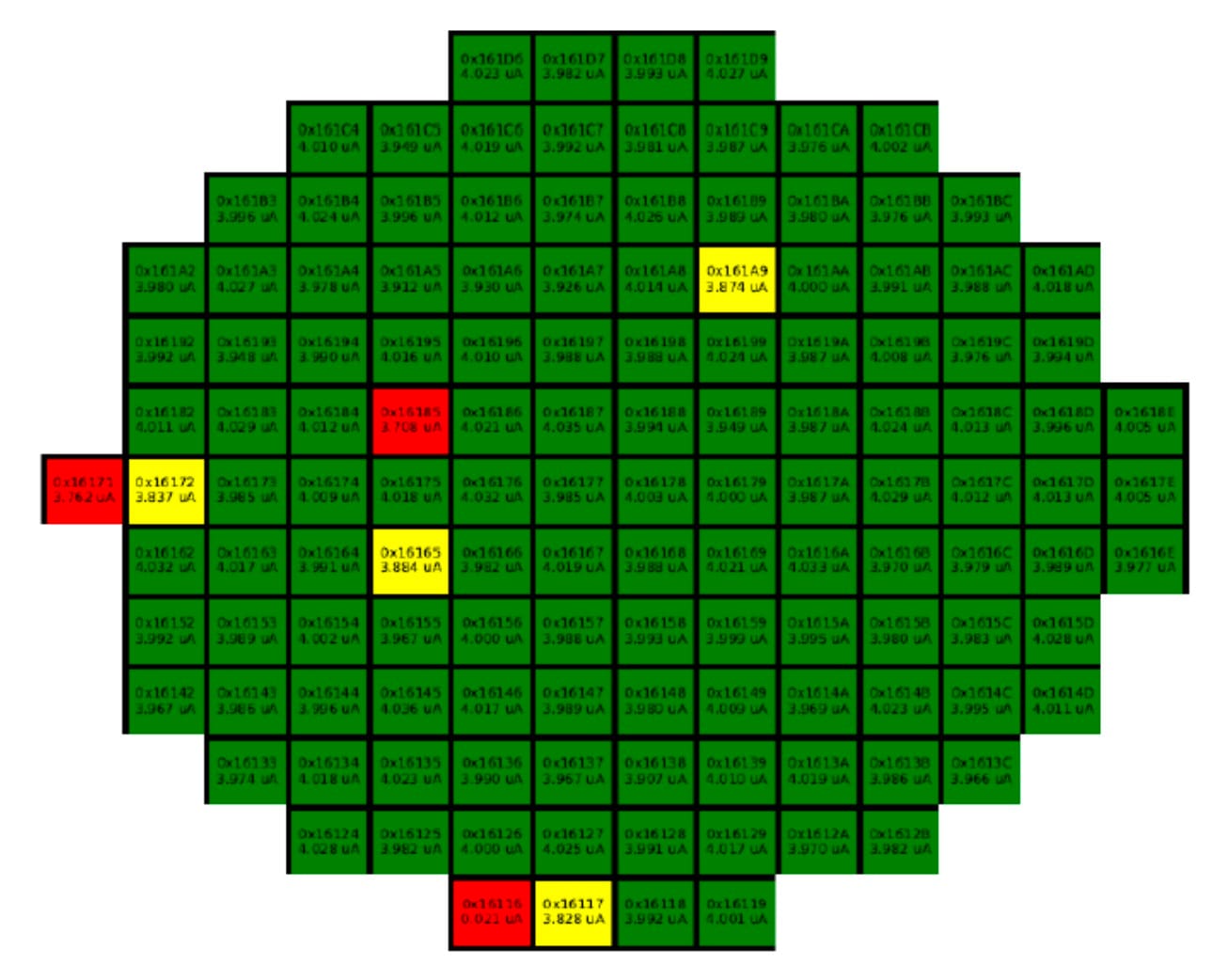
Finally, results of the analysis have to be presented both numerically – for long-term storage in the central database of the CMS experiment, and visually – for quick and easy inspection by eye, to understand the quality of the chip and validate the test itself. The most important outcome of these tests is a coloured wafer map clearly marking the good chips that a dicing company should then collect for the next stages of the detector assembly.
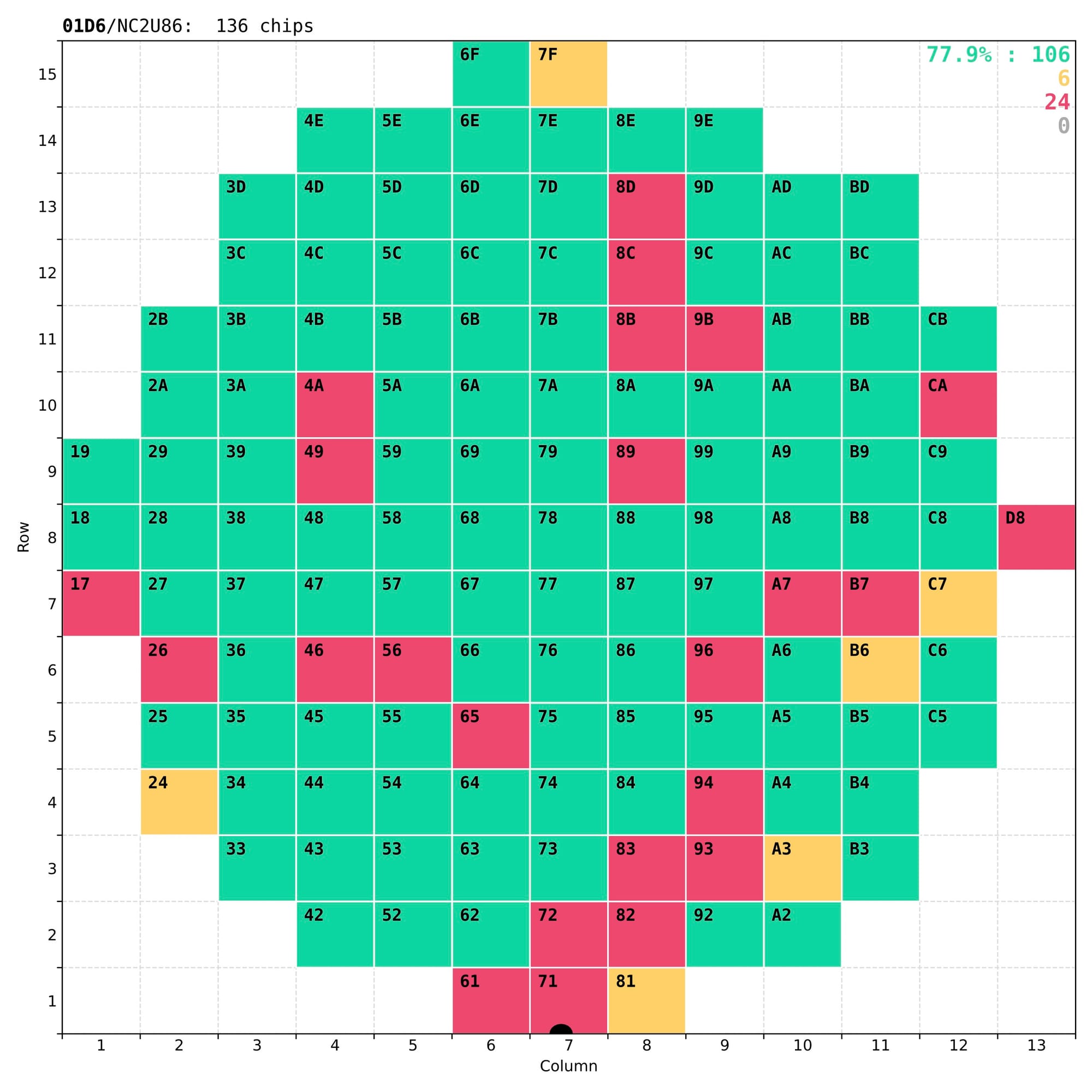
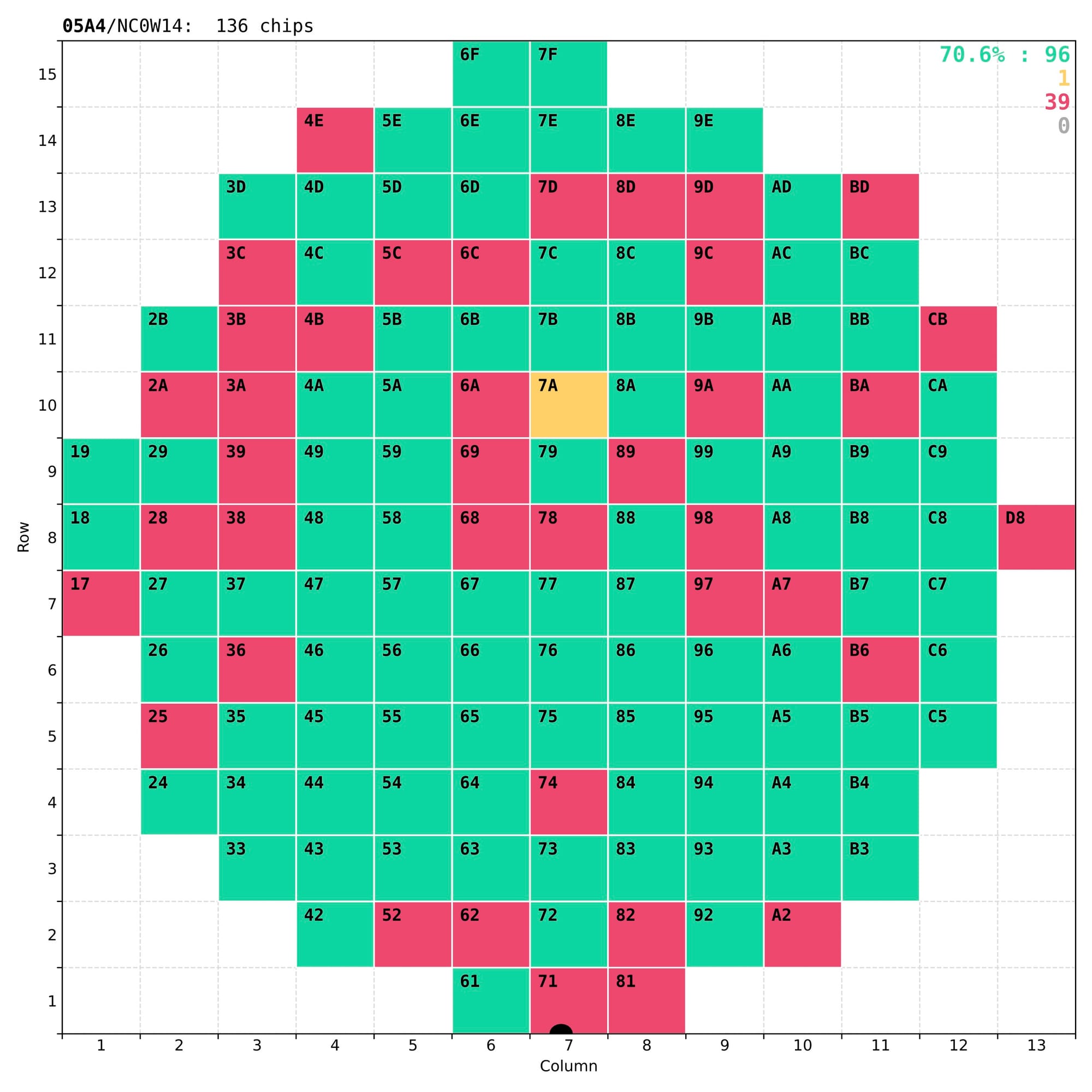
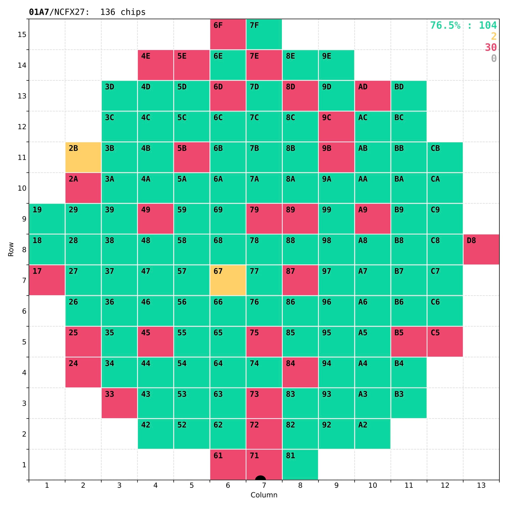
Examples of wafer maps sent to the dicing company together with the tested wafers, with typically 70-80% of good chips.
In reality some of the less-good chips that have non-critical defects (marked as yellow) are kept for other applications, either in the laboratory or in other experiments.
Technical implementation
As a starting reference I've used the plots produced by another team for an earlier version of this chip, code-named RD53A. It already had several features that we wanted to replicate:
- colour-coded wafer maps displaying the quality grades for every chip;
- 1D distributions of single-test chip metrics across quality regions;
- detailed analysis plots for complementary tests in single chips.
Sample visual presentations of the results from earlier tests of the RD53A chips
To provide the necessary flexibility and easy configuration of individual plots, I've decided to build the analysis code in Python, which also made it easier to integrate with the rest of the testing and control setup, written in Python as well.
Output format
After reviewing in detail every use case for the results of these tests it was decided that PDF is the optimal output format. These were the main reasons:
- its wide adoption by all the major operating systems and web-browsers means that anyone can open it without the need for special software;
- it supports vector graphics that allows to preserve high-precision details of the distributions while maintaining small file size;
- it supports pagination, that matches naturally the large number of tests that can be combined into a single file to simplify book-keeping;
- it supports text search, enabling quick navigation to the test of interest.
In addition, all the output is also written as JSON files, from which the numerical values are extracted for further statistical analysis across multiple wafers and for long-term storage in the database.
Key technical aspects
The major part of the analysis code has been divided in two modules:
- chip-level – produces individual plots in PDF format for every input file with raw data based on the list of plot configurations;
- wafer-level – propagates the analysed data and chip-level plots to the wafer map to produce the final output in the context of the whole wafer.
A number of libraries are used under the hood:
- matplotlib – to draw all the visualisations and data distributions with low-level control over every detail;
- numpy – to perform numerical calculations, linear and gaussian fits of data points, etc.
- PyPDF2 – for composition and low-level manipulation of PDF files;
- ROOT – for reading and advanced statistical analysis of the high-volume raw data coming from the data-acquisition system.
To enable concise and flexible plot definitions I've implemented a custom template system that mostly relies on dictionaries, lambdas and predefined utility functions. These configurations can range from fairly simple ones, which constitute the majority of the plots:
'iina_shuntldo_start': {
  'input': 'power_startup_shunt/IINA',
},
'ana_r_shuntldo_start': {
  'input': 'power_startup_shunt/R_ANA',
  'db': {
    'R_SLDO vector': lambda o: {-1: o}
  }
}
to several complex ones with multiple sets of data points calculated on the fly:
'drop_iv_shuntldo': {
  'input': COMMON_OUTPUTS['drop_iv_shuntldo']['input'],
  'output': {
    key: value for dic in [COMMON_OUTPUTS['drop_iv_shuntldo']['output']] + [
      {f'+fit_{name}':  lambda i, o, n=name: fit_pol(o[n], sigma=i['+err_gnd'] if 'GND' in name else '+err')
      } for name in [
        'VIND', 'VINA', 'GND', 'GNDD', 'GNDA1', 'GNDA2',
    ]] for key, value in dic.items()
  },
  'output_sum': {
    key: value for dic in [{
      f'o_{name}': lambda o, n=name: o[f'+fit_{n}'][0][0],
      f's_{name}': lambda o, n=name: o[f'+fit_{n}'][0][1],
      f'c_{name}': lambda o, n=name: o[f'+fit_{n}'][1],
    } for name in ['VIND', 'VINA', 'GND', 'GNDD', 'GNDA1', 'GNDA2']] for key, value in dic.items()
  },
  'text': [
    f'{name.replace("_", " ")}:  O: {{o_{name}:.3f}}  S: {{s_{name}:.3f}}  $\chi^2$: {{c_{name}:.3f}}' for name in [
      'VIND', 'VINA', 'GND', 'GNDD', 'GNDA1', 'GNDA2',
    ]
  ],
  'fit.draw': {'+fit_VIND':  0, '+fit_VINA':  1, '+fit_GND':   2, '+fit_GNDD':   3, '+fit_GNDA1':   4, '+fit_GNDA2':   0},
  'title': 'Voltage drop (SLDO) [{chip_column:X}{chip_row:X}];Current [A];Voltage [mV]',
  'axis.range': ((0.8, 2.2), (0.0, 120)),
  'legend': None,
  'legend.loc': 'lower right',
  'group': 16,
}
The code examples above define the logics of the plots, which are defined one by one in a single Python file (over 2300 lines). Each piece of configuration supports multiple styling parameters, such as axis titles and ranges, legend definition, etc., which are then translated into low-level commands for matplotlib.
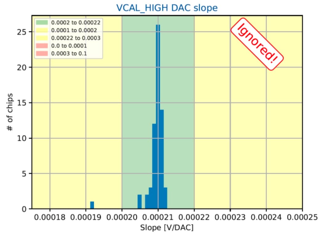
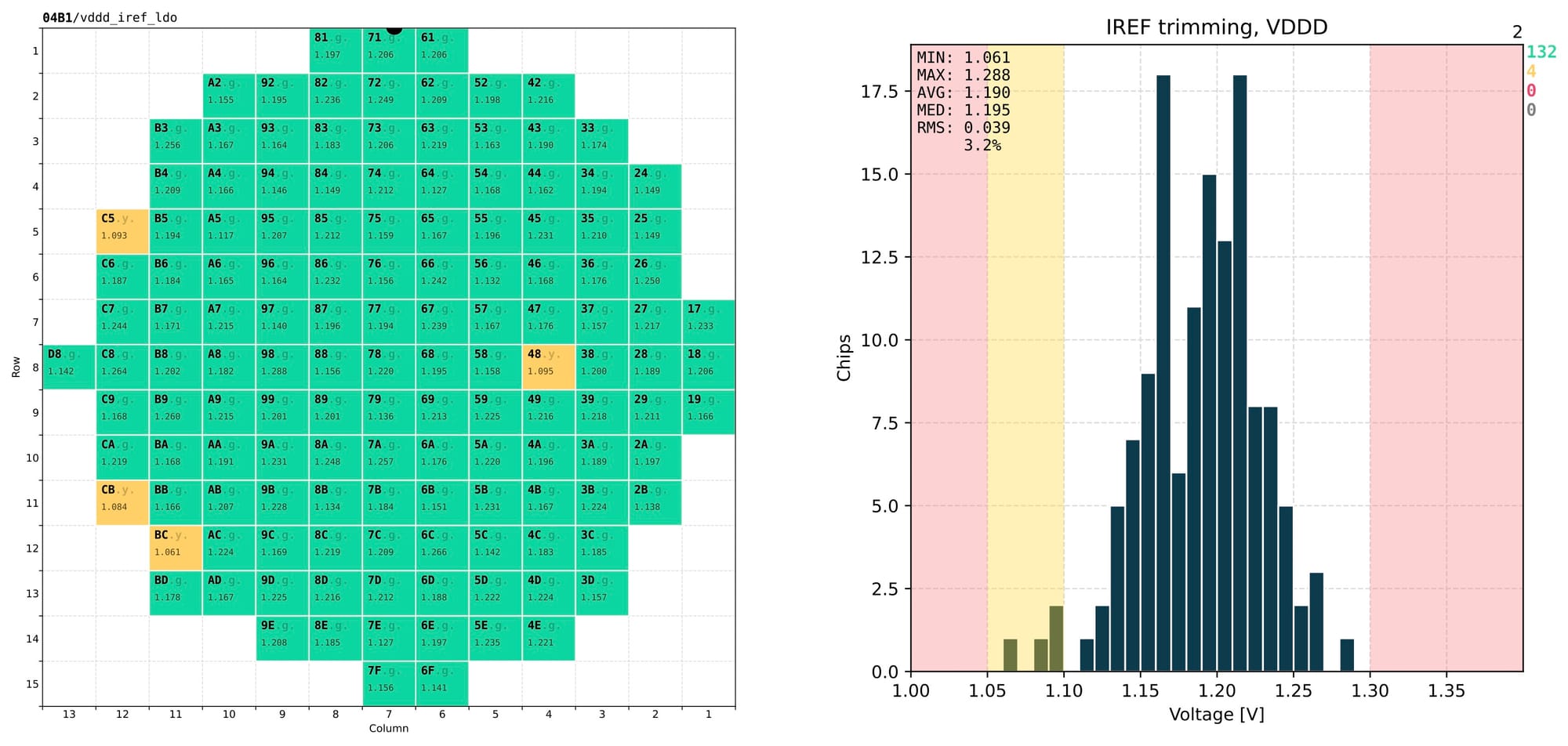
Another piece of configuration is defined only for wafer-wise plots that have exactly 1 entry per chip. This configuration defines the boundaries of quality regions, binning, axis titles and other book-keeping information organised in 1 line per plot:
"iind_vddd_ldo":    ([0.55, 0.65, 0.65, 0.72, 0.72, 0.83 ],  5e-03,  5,  1, "Digital current [IREF+VDDD trim] (LDO);Current [A];Chips"),
"offset_vddd_ldo":  ([0.70, 0.86, 0.90, 1.10, 1.14, 1.30 ],  2e-02,  5,  0, "VDDD trimming (LDO);Offset [V];Chips"),
"slope_vddd_ldo":   ([18, 21, 21, 27.5, 27.5, 30         ],  4e-01,  5,  0, "VDDD trimming (LDO);Slope [mV/code];Chips"),
"global_registers": ([0, 0, 0, 1, 1, 10                  ],  1e+00,  6,  1, "Global registers;# of failed registers;Chips"),
"capacitance_inj":  ([7, 7.2, 7.2, 8.8, 8.8, 9.7         ],  1e-01,  7,  0, "Injection capacitance;$C_{inj}$ [fF];Chips"),
This code layout allows to keep the visual part of the plots separate from the calculation and plotting logics. They defined in different files of a GitLab repository, simplifying the tracking of changes as we adjust or add new quality criteria. The boundaries of quality regions for each plot are defined by 6 values inside the square brackets: [🟥🟨🟩🟨🟥]. This convention allows to exclude some regions by reusing the same number for several boundaries in a row.
Finally, in order to speed up the analysis in the middle of an ongoing wafer test, I've imlemented caching of the relevant numeric data from the previously analysed chips using the pickle module. This doesn't avoid redrawing of the plots and wafer maps after every tested chip, but it does save the time spent on reading and analysing the raw data.
Visual design
Visual representation of the analysis results have to be clear, concise and functional. My goal was to present the large amount of data from a single wafer in the most user-friendly way, while staying within the constraints and capabilities of the PDF format.
Use cases
A number of distinctive use cases had to be covered, both in the process of defining the relevant quality criteria and later, during the daily testing of hundreds of wafers at the production stage. Here are some of the most common use cases that I kept in mind:
- ensure that all chips have been tested successfully;
- see the yield of good chips in the tested wafer;
- find the exact measured value from a specific test in a specific chip;
- identify the tests responsible for invalidating most of the chips;
- for a specific chip find the test responsible for its bad quality grade;
- evaluate the spread of a specific measurement across the chips in a wafer;
- detect outlier chips for closer look into their behavior.
General layout
I've adopted a fixed layout for the output PDF file, with 1 page per measurement. Each page is divided in two sections:
- left – shows a wafer map with relevant information about every single chip;
- right – aggregated distribution of the measured values with the relevant statistical information.
This layout allows to instantly evaluate the quality of a specific test from just one page and skim quickly through many pages and spot any obvious issues.
To simplify navigation through the 100+ tests, a summary page is added at the beginning of the output PDF with a slightly different layout:
- left – wafer map showing the overall quality or testing status of every chip;
- right – a stacked histogram with every bar representing a single test, showing the counts of chips that have or have not passed that test.
Overall status of a chip is defined as the lowest quality level that the chip has in any of the tests marked as critical. For example, if a chip falls into the yellow band for any of the critical tests, it is graded as yellow, even if it appears as green in all the other tests.
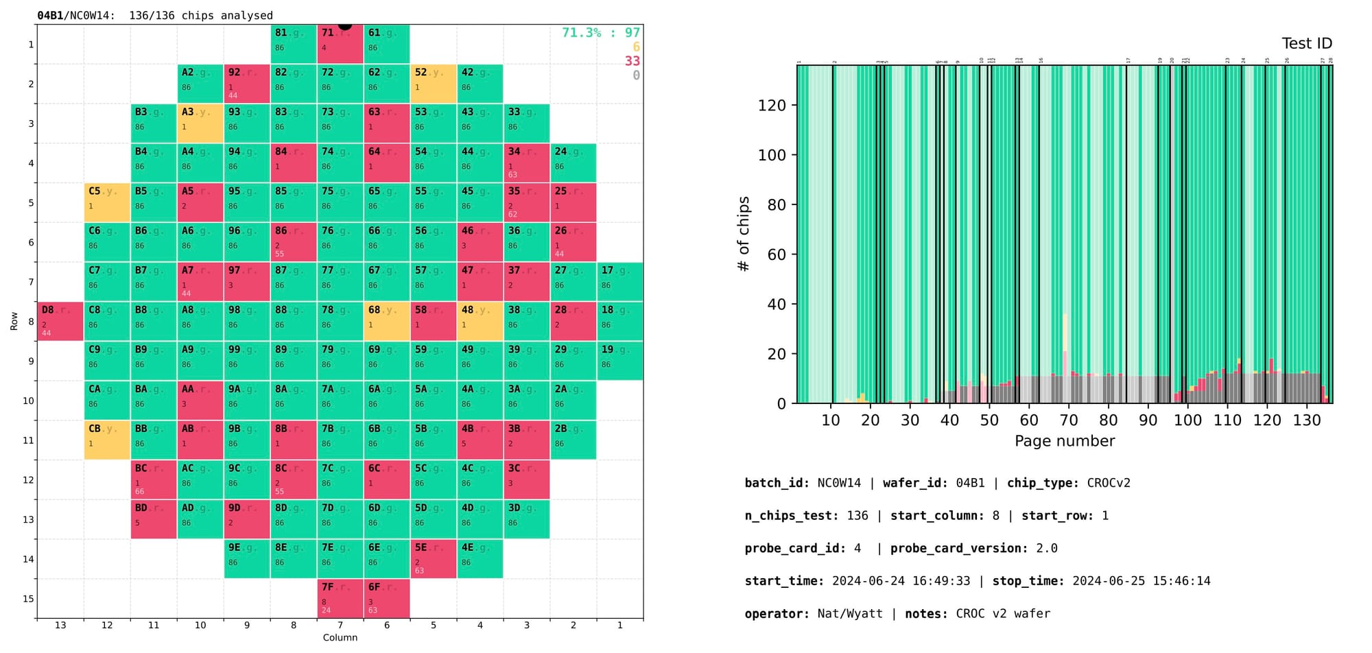
Complementary tests that are not used for chip rejection are marked with semi-transparent overlay bars in the right section of the summary page. Groups of related tests are separated by solid black lines marked with numeric group IDs at the top. Page numbers on the X axis allow to quickly locate the page with that test.
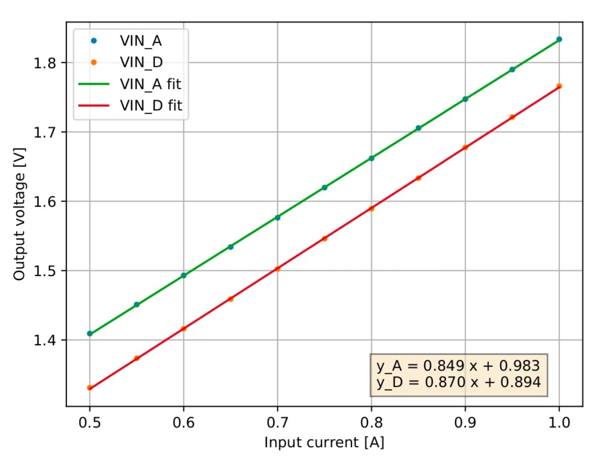
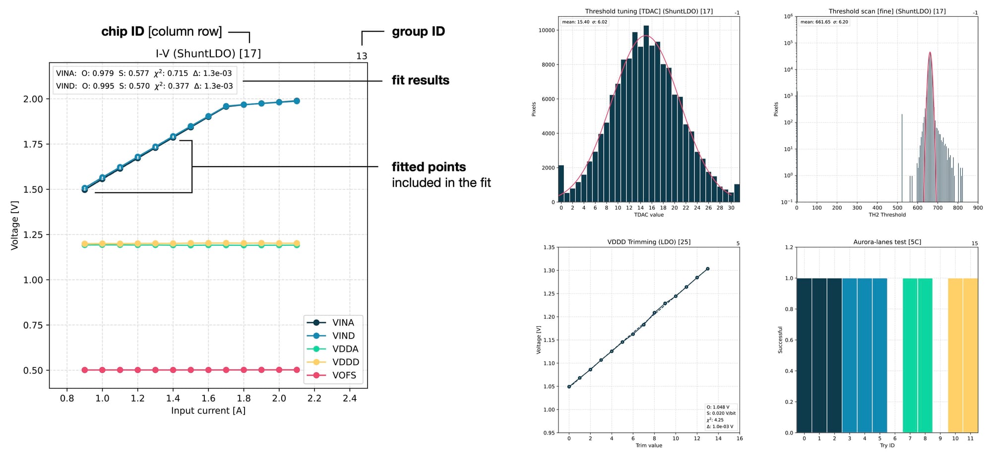
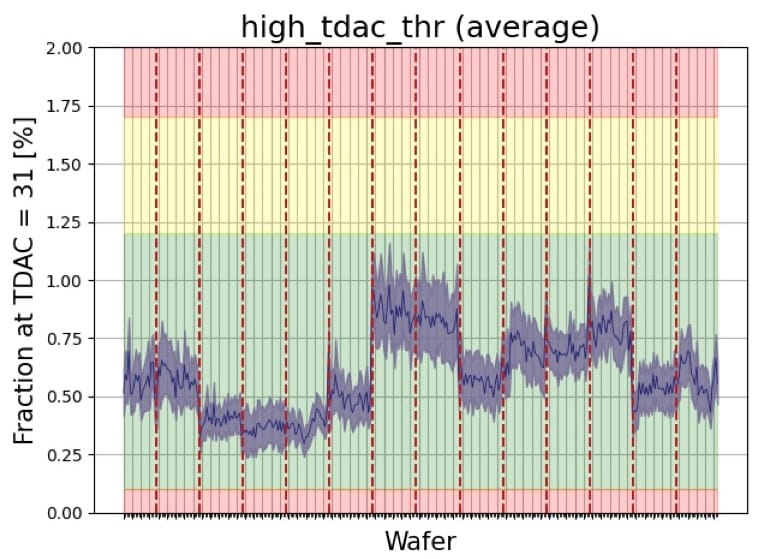
Finally, a number of in-depth plots are produced for detailed examination of various parameters of the chip. These plots are produced for individual chips and usually have more complex configurations. They can show multiple sets of points or even tens of thousands of values, like during threshold or noise scans that measure every single pixel in a chip. Here are a few examples of such plots that are used for deeper investigations.
Design details
There are many small details in this layout that enable the use cases mentioned earlier. Apart from the generally clean and minimalistic aesthetics for easier interpretation of the results, here are the few details that might be less obvious.
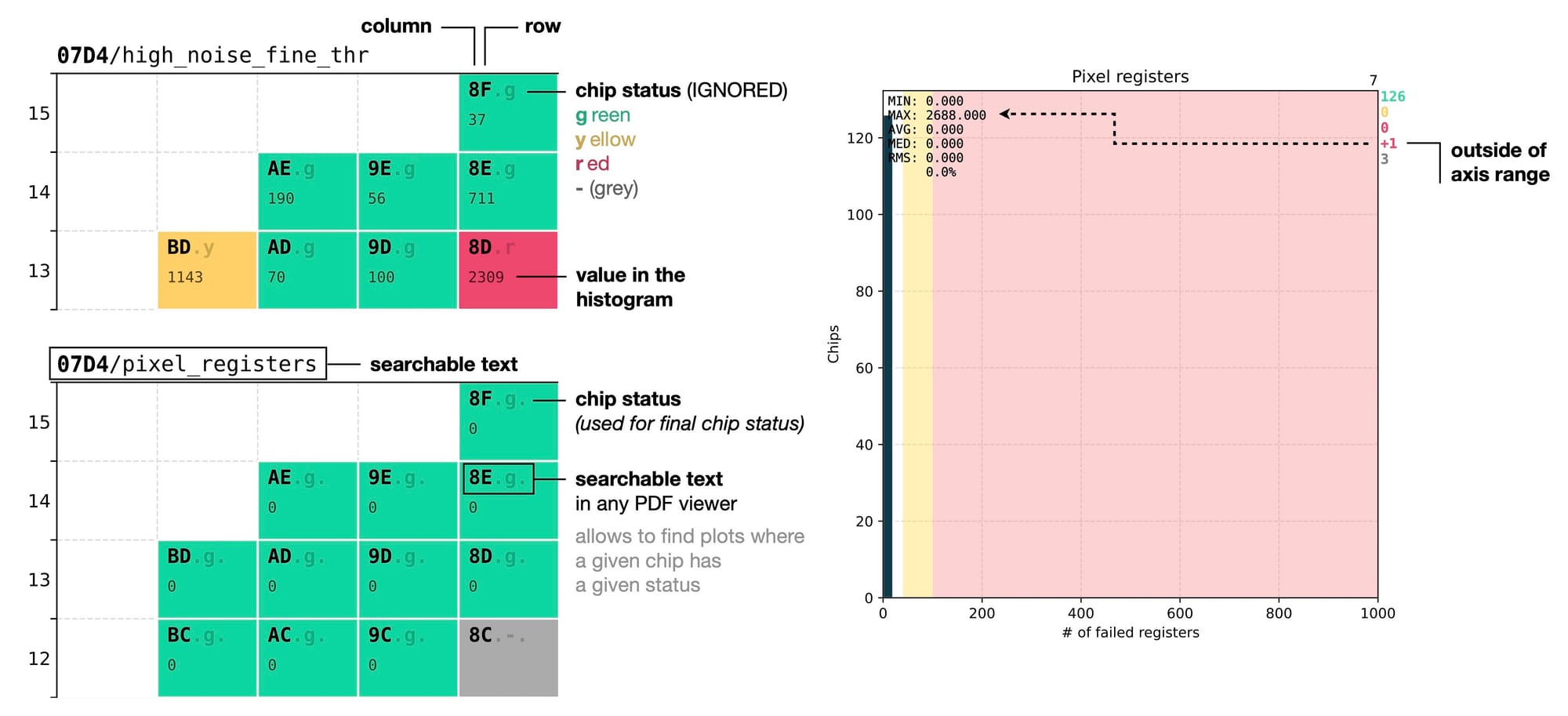
The wafer map uses 5 distinct visual styles for drawing a chip based on its status:
- filled green – good chip, which is safe to use in production;
- filled yellow – functional chip with some defects, which can be used internally in the lab;
- filled red – chip with critical defects that can't be used for anything;
- filled grey – chip that was tested in general but doesn't have the data from this particular test (for example because it was interrupted by an earlier failure);
- dashed grey – chip that has not been tested at all.
In the plots with chip distributions I've removed green background from the good-quality section, leaving it white. This creates visual focus on the main area of interest and reduces distraction by too many colours.
I've used subtle dashed lines of light-gray colour for the grid to not interfere with the actual distributions of interest, while being visible enough when they are needed to compare different regions of the same plot. Instead, in the wafer map I've used solid white lines for the borders to make clear visual separation between the chips.
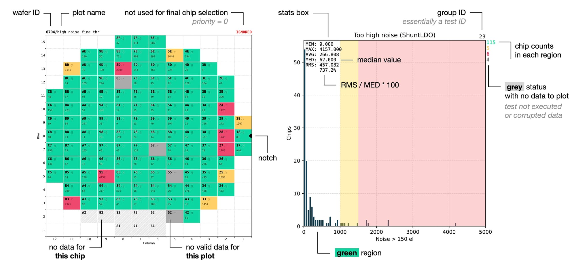
Colour-coded chip counts for every quality region complement the visual distributions and the wafer map, using the same colours as the wafer map for an immediate visual connection between the two. A separate red line with a +N is added for chips falling outside of the X-axis range, making it easier to spot outliers.
The statistics box shows several values for better understanding of the distribution. In particular the minimum and maximum values give the idea about the position of the outliers on the X-axis, which can then be located in the colour-coded wafer map by combining the red colour with the exact numerical value. Monospace font and 3-letter abbreviations are used for vertical alignment of each line, giving it a cleaner look.
Looking into more details, every wafer map has its wafer ID followed by the test name written at the top. The wafer ID is repeated on every page to clearly distinguish results from different wafers. This is helpful to avoid confusion in cases when several PDF files with results from different wafers are opened side by side for a comparison.
Every chip ID is written in bold monospace font to be clearly visible regardless of the drawing style of the chip, as it is the first piece of information that we try to locate. It consists of two characters representing the column and row position on the wafer in hexadecimal format.
This is a convenient choice thanks to the fact that the wafer layout is divided into 12 x 15 dices, with both numbers fitting within the range of the hexadecimal system. This allows to define the position of a chip with only 2 characters instead of 4 (if we used the decimal system), making it faster to read.
Chip ID is followed by a dot and a status letter that represents the grade of the chip in the current context. Another dot after the status letter is added if the test is actually used for quality rating. It provides a concise textual representation of the chip quality, complementing its colour in the wafer map, and is included both on the summary page and on the page of every test.
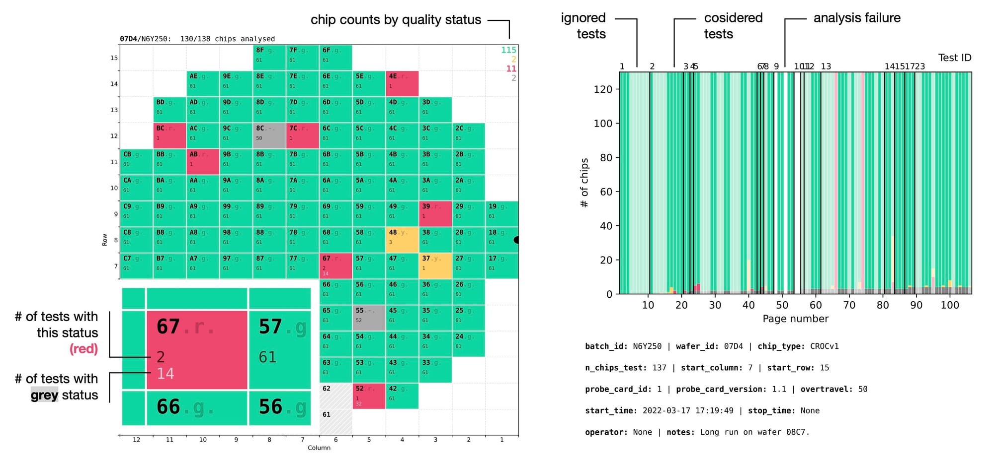
This allows to use Search function in any PDF viewer to quickly find a test failed by a specific chip. For example, when you see a red chip labeled as 67.r. with number 2 underneath, it means that out of all the analysed tests this chip appeared as red in two of them. Searching for 67.r in the document will immediately reveal the two other pages where this chip is red, allowing to quickly understand whether it is a real problem with the chip or some edge case, for example suboptimal quality thresholds for those particular tests.
Like with the grid lines, the status letter had to be subtle. It should be readable enough to find it when necessary, but faint enough to not distract from the key information, which in 99% of the cases is the chip ID. After all, the chip status is communicated much better by the colour, not by text. To achieve this I've implemented the chip label as two layers on top of each other:
- semitransparent label with the full string: 67.r.
- fully opaque label with only the chip ID: 67
Results
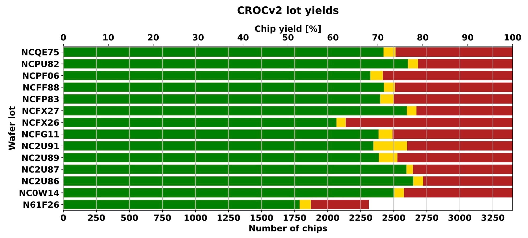
As of today, all the 345 production wafers with almost 47K chips have been successfully tested and analysed using the setup I've described. This large number of chips was produced across 14 separate batches that showed small variations in certain parameters and in quality of the chips. The average yield of the good chips has been around 72%, which are now used for assembly of the detector modules.
Results summary from a presentation by Michael Grippo (2026)
You can find more information about the project and the technical team behind it, including Michael Grippo, who developed most of the control and testing code, in this brief news article at the CMS website:
And as a bonus, here is a video of the automated wafer-alignment process based on the pattern-recognition functionality of the FormFactor probing station, which I've recorded in our cleanroom. The precision of its positiniong system is quite impressive.